Hardware as Code: How AI Agents Built My CO2 Monitor
In Part 7 I mentioned, almost in passing, that I didn’t type most of the new board myself. This post is about how that actually worked.
Some context: I’m a software engineer, not a hardware engineer. Before this, my only PCB was the module carrier board from Part 6, drawn by hand in EasyEDA. Now there’s a board on my desk that JLCPCB assembled from files that AI agents generated, running firmware that was tested before the board existed. The project finally has a name too: StuffyMeter.
The short version: AI agents became useful for hardware once the hardware became code. I built all of it with AI agents in Antigravity, Google’s agentic development platform.
Why code instead of a CAD program
Agents are good at text. They can read and edit code, run a command, read the output and try again. Clicking through a CAD program is a different story. KiCad, the free PCB tool, has a command line interface and a Python API, so everything a person would do in its GUI can be a script instead:
- the circuit is a Python file
- scripts turn it into a KiCad schematic and a board
- every check (electrical rules, design rules, part placement, simulation, case fit) prints a report
Once that’s true, building hardware looks a lot like building software. The agent edits code, runs the pipeline, reads the reports, and fixes things until everything passes. I get diffs I can review, and a design I can rebuild from scratch with a few commands.
The board is a Python file
Everything starts with design.py. It has two parts. The first is a catalogue: for each kind of part, what to buy and how it’s drawn and soldered.
# Part catalogue (simplified)
'ME6211': Part('ME6211C33M5G-N',      # value
    'Regulator_Linear:ME6211C33M5',   # schematic symbol
    'Package_TO_SOT_SMD:SOT-23-5',    # PCB footprint
    'C82942', ...),                   # JLCPCB part number
The footprint is the copper pad pattern the part gets soldered onto, and the part number is what JLCPCB actually buys and places.
The second part lists every component and maps each pin to a net. A net is just a name for a wire:
add('U4', 'ME6211', {'1': 'VSYS', '2': 'GND',
                     '3': 'LDO_CE', '5': '+3V3_SENS'})
add('R14', 'R_100k', {'1': 'SENS_EN', '2': 'LDO_CE'})
add('U1', 'ESP32C3', {..., '16': 'SENS_EN', ...})
There are no wire coordinates anywhere. Pins that share a name are connected. Here, pin 16 of the ESP32 (SENS_EN) goes through R14 to the enable pin of U4 (LDO_CE), the regulator that powers the sensors, so the firmware can switch the sensors off and on again. A script turns this into a normal KiCad schematic, where matching labels mean the same wire:
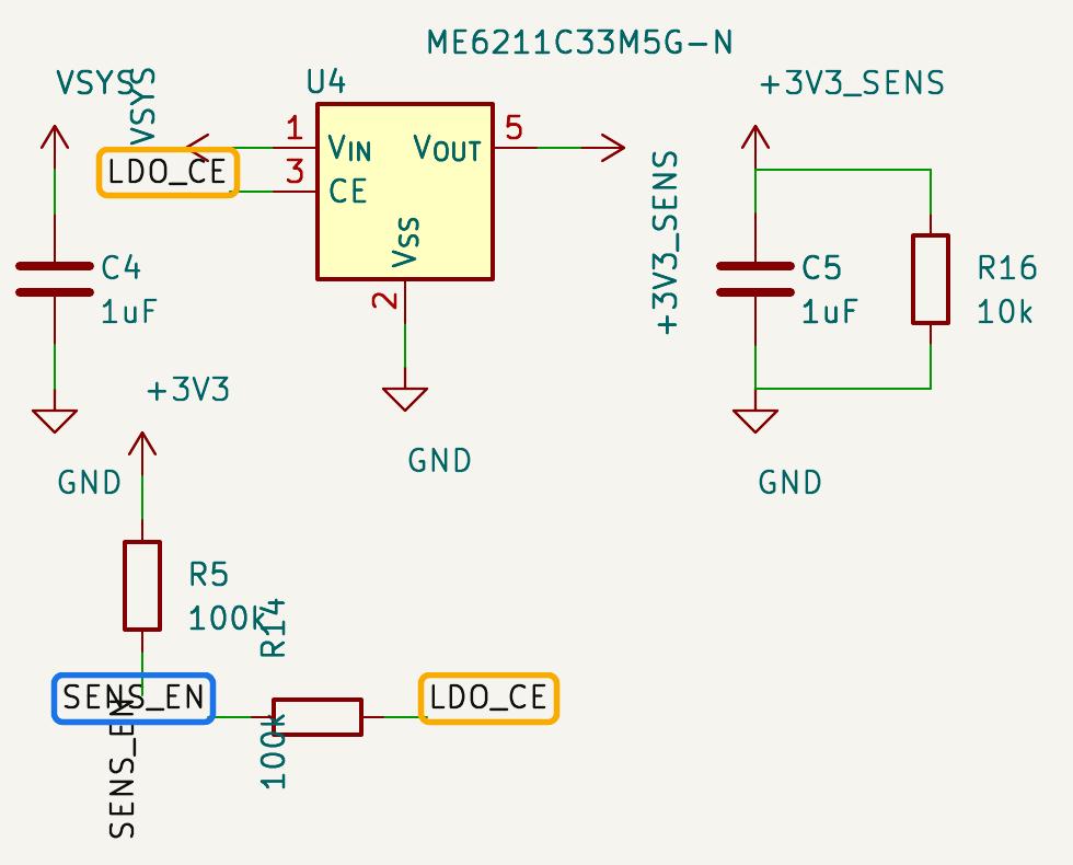
The battery version of the board is 104 components and 55 nets in 441 lines of Python. The agents also write the reasoning next to the parts as comments. That enable pin, for example, must never go above the regulator’s input voltage plus 0.3 V, and the comment explains how the 100k resistor keeps it safe when the battery runs low. When I come back to the file later, the why is right next to the what.
From Python to factory files
One pipeline turns that file into the three files JLCPCB asks for: the Gerbers (one image per copper, solder mask and silkscreen layer), the BOM (which part goes where) and the CPL (the x, y and rotation of every part for the pick-and-place machine).
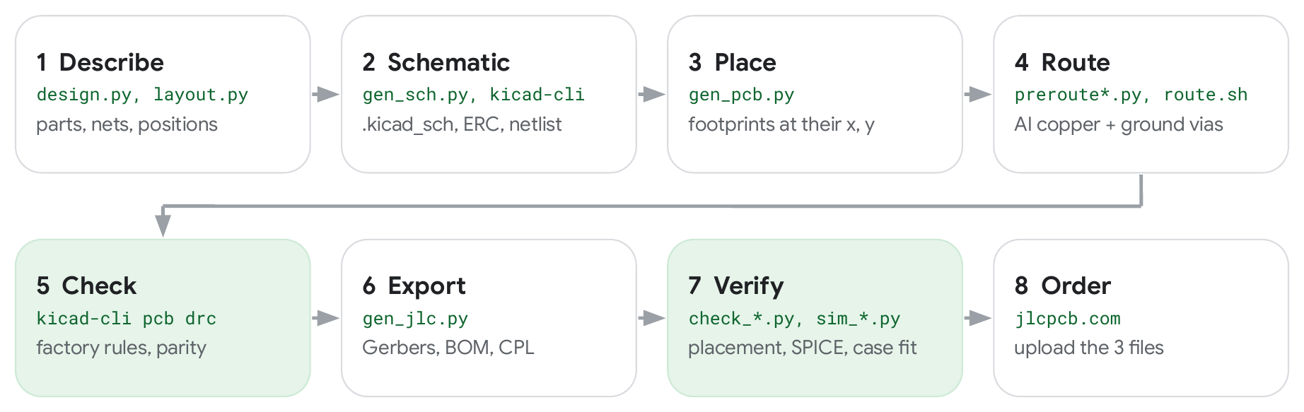
KiCad 10 runs headless in Docker, so the whole thing is a handful of commands, like a CI job:
# schematic, then ERC and a netlist with kicad-cli
./kx.sh python3 /work/gen_sch.py
# place, route, design rule check
./pipeline.sh 8
# Gerbers, BOM and CPL, then the placement check
./kx.sh python3 /work/gen_jlc.py && python3 check_cpl.py
A second file, layout.py, holds the physical side: the board outline, the mounting holes and the position of every part. The case is code too, written with build123d (a Python CAD library). It reads the same layout, so when a connector moves, the opening in the case moves with it.
Routing: I expected an auto-router, the agent wrote the traces
Routing means drawing the copper traces between pads. My plan was to let Freerouting, an open source auto-router, do it. On an earlier, smaller revision of this two-layer board, it gave up with seven nets still unconnected, every single try.
What worked was having the agent write every signal trace as data: a net, a width, a layer and a list of points, plus the vias that hop between the two layers.
# net, width (mm), layer, points (mm)
('+3V3', 0.4, 'F', [(31.95, 12.75), (33.35, 14.3)]),
('GND', 0.4, 'F', [(31.45, 14.3), (30.2, 14.65)]),
# via: net, x, y, diameter, drill
('GND', 33.3, 11.2, 0.7, 0.4),
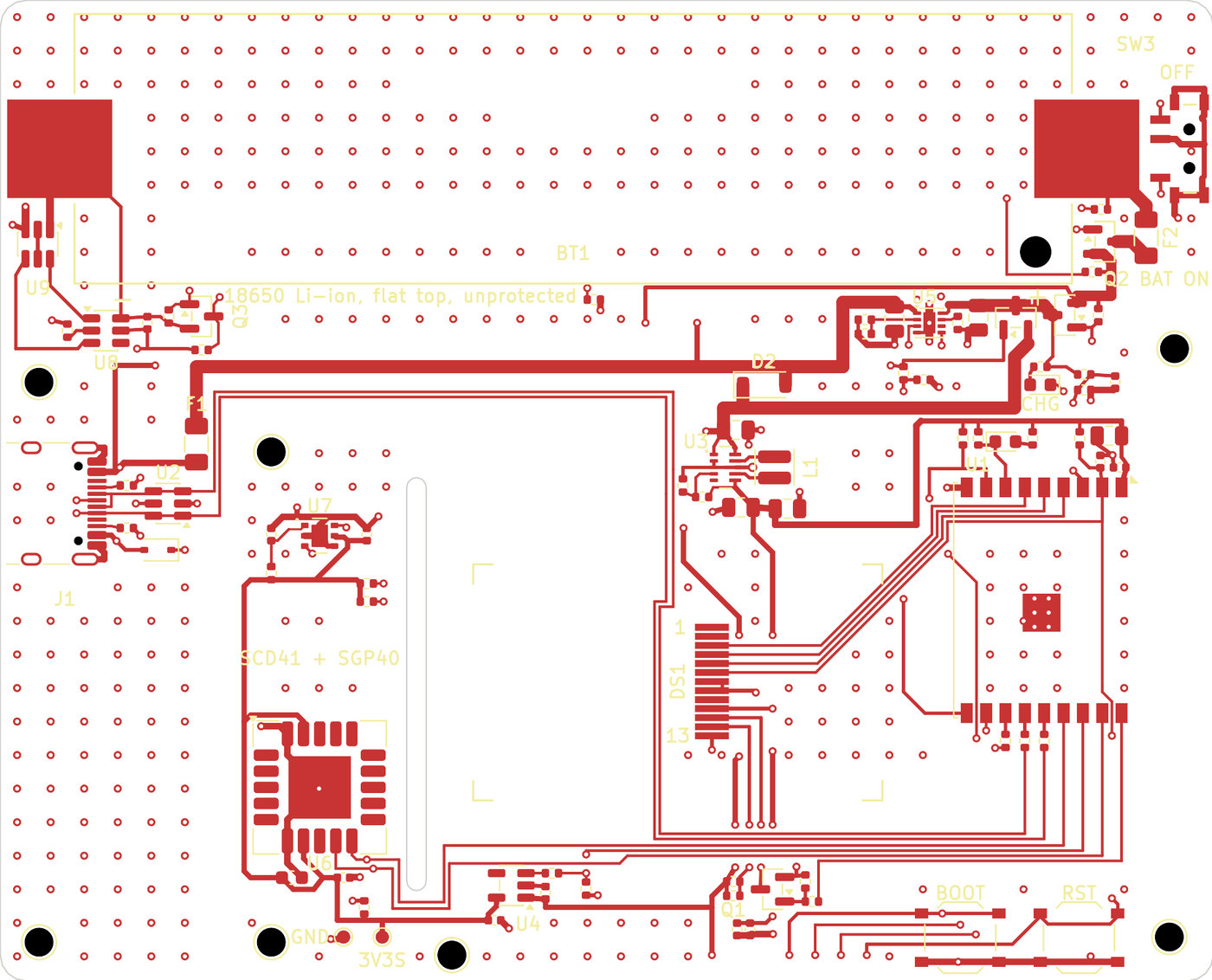
Those traces are locked. Freerouting is now only allowed to connect ground pads to the ground plane, and copper pours fill the empty space with ground. The battery board’s routing is 665 lines of this, and the design rule check ends with zero violations and zero unconnected pads.
The checks are the test suite
This is what makes the whole thing trustworthy. Hardware mistakes are expensive: a bad board costs money and a few weeks of waiting. So every change re-runs every check, and each one maps surprisingly well to something from software:
| Check | In software terms | What it caught |
|---|---|---|
| Live part search (JLCPCB API) | dependency resolution | The SGP30 I used in V1 is discontinued, so the board uses an SGP40 |
| ERC, DRC, schematic parity | type checker, linter | After a pin swap, a stale hand-written trace shorted 3.3 V to ground |
| Placement (CPL) check | deployment test | A drop-in alternative charger chip sits 90° rotated in JLCPCB’s library |
| SPICE simulation | unit tests | The USB back-feed below, before and after the fix |
| Case fit check | integration test | A fuse’s 3D model was 0.54 mm tall, the real part is 1.6 mm |
| Independent AI review | code review | NO-GO twice before ordering |
The placement check is a good example of why this matters. JLCPCB’s machines use their own footprint library, and a footprint there can be rotated differently from KiCad’s. If the CPL file doesn’t account for that, a chip gets soldered on turned 90 degrees. check_cpl.py places JLCPCB’s version of every footprint at the CPL position and compares every pad with the KiCad board. Anything more than 0.05 mm or 0.5° off fails. On the battery board, all 81 parts land at 0.000 mm.
What the AI got wrong
The agents made mistakes, sometimes with a lot of confidence. Three examples:
- An agent once told me JLCPCB had no 18650 battery holders at all. Its search was bad: “18650 holder” only matched empty placeholder listings. Searching for “18650” found holders with thousands in stock.
- In rev 3.0, the display footprint (copied from a library) used the flex cable’s unfolded length. The cable is meant to be folded, so the screen would have ended up about 2 mm off, and the soldering note would have mirrored the pins. The reviewer caught both.
- In the battery version, the design agents missed that the ESP32 keeps its USB pull-up on while running from the battery. That 3.3 V leaked through the USB protection chip and lifted the USB power line to about 1.8 V in simulation, so the firmware couldn’t tell whether USB was plugged in. One small diode fixed it. With it, the line stays at 0.01 V.
None of these made it into an order. That’s what the checks are for, and the reviewer: an agent that designed nothing and only reads the finished design, looking for problems.
Firmware before the hardware existed
The firmware has the usual hardware problem: the board isn’t there yet. So I used QEMU, which emulates the ESP32-C3. The real firmware image boots on my PC, with its web API, OTA updates and MQTT. But QEMU knows nothing about my sensors or my battery, so the QEMU build swaps those drivers for models.
The CO2 model is simple. When people are in the room, CO2 climbs toward 1,900 ppm. When the room is empty, it decays back to the outdoor level of about 430 ppm, with a time constant of seven minutes. This is the real model code, run for three simulated hours:
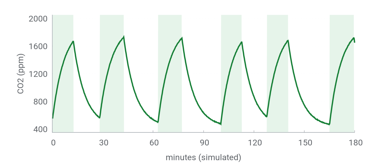
The simulated sensors keep the timing of the real ones: a CO2 reading every 5 seconds (every 30 in low-power mode) and the VOC sensor’s 46-second warm-up. A test can also make a sensor stop answering, and the firmware has to go through the same recovery steps it uses on the real board: reset the I2C bus after three failures, power-cycle the sensors after five.
The battery is a model too. In the QEMU build, the battery voltage and the USB state come from a test hook instead of the ADC, so a test can unplug USB and drain the cell:
inject(api, usb="off", vbat=3.85)
until_state(api, "battery", volts=3.85)
inject(api, usb="off", vbat=3.25)
until_state(api, "empty", 60)   # low-battery cutoff
inject(api, usb="on")
# expect a clean restart with last_reboot == "low_battery"
The network, an MQTT broker and the update server are faked as well. QEMU can’t drive the display, so the screens are rendered on the PC from the same UI code. Firmware 1.0 was written this way while the boards were still on their way, and as I wrote in Part 7, it mostly just worked when they arrived.
How the agents worked together
For the earlier boards I mostly worked with one agent at a time, plus a separate reviewer before ordering. For the battery version I ran a small team:
- a coordinator agent that split the work and kept a shared spec (the decisions, the ESP32 pin map, the metrics) that everyone built against
- separate agents for the PCB, the firmware, the case and the monitoring stack, each in its own git worktree
- a reviewer that hadn’t designed anything, with one job: say GO or NO-GO
Every agent worked in the same loop:
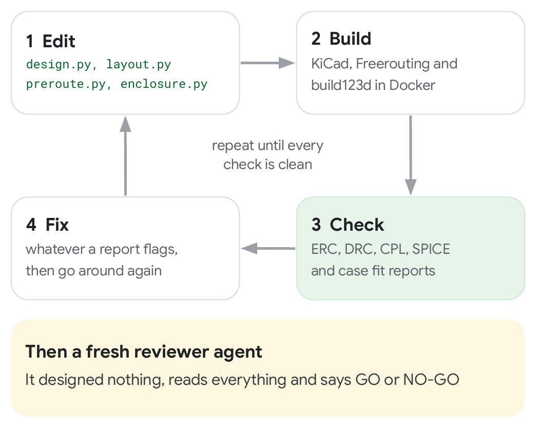
The battery version (a charger, cell protection, a bigger board and a new three-part case) took about a day from the approved plan to a release. My job was the part an agent can’t decide for me: what I want, the trade-offs (a replaceable 18650 cell instead of a LiPo pouch, a printed button that’s easy to press, a switch that disconnects the battery), and the final approval.
What I learned
- Make everything a command with a report. If a step needs someone to click through a GUI, the agent can’t close the loop.
- Give the agent numbers to hit: zero ERC errors, zero DRC violations, every part within 0.05 mm, every simulation case passing. “Looks good” isn’t a test.
- Don’t trust a single source. Library footprints can be wrong, and JLCPCB’s library doesn’t always agree with KiCad’s. Check one against the other.
- Use live data for parts, and still sanity-check the query.
- Get a second opinion from an agent that didn’t build it. It found things the design agents were blind to.
- Simulate what you can’t test yet. SPICE for the circuit and models in QEMU for the firmware found real bugs before any hardware existed.
None of this replaces understanding what you’re building. I still read the reports and the reviews, and I asked a lot of “why” questions along the way. But I’m a software engineer with a factory-assembled board on my desk, and I don’t think I’d have gotten here this quickly any other way.
What’s next
The battery version is designed, simulated and reviewed, but not built yet. I’ll write about it once the boards arrive.
I work at Google, which makes Antigravity. StuffyMeter is a personal side project, and the opinions here are my own.