DIY Smart CO2 Monitor Part 6: Custom PCB Design and Manufacturing
After successfully miniaturizing our CO2 monitor with a 3D printed enclosure in Part 5, it was time to tackle the final stage outlined in our original roadmap: Stage Three - Custom PCB & Cost Optimization for Potential “Mass Production”. What I discovered during this journey was that custom PCB design and manufacturing is far more accessible and affordable than I ever imagined!
The Discovery: JLCPCB and the Modern PCB Ecosystem
When I first outlined this project in Part 1, I thought custom PCB manufacturing would be expensive and complex. After some research, I discovered JLCPCB - a game-changing service that offers:
- Custom PCB Manufacturing: Professional-grade PCBs at incredibly low prices
- Bill of Materials (BOM) Management: They can source and purchase components
- PCBA (PCB Assembly) Services: End-to-end assembly for complete prototyping
- EasyEDA Integration: A free, web-based PCB design tool
The combination of affordable manufacturing and accessible design tools has truly democratized hardware development for individual makers like myself.
Step 1: Schematic Design with EasyEDA
The first step was creating a circuit schematic using EasyEDA, JLCPCB’s online PCB design tool. What impressed me most was how comprehensive their component library is - I could easily find all the components I was using:
- NodeMCU ESP32 Development Board
- SCD41 CO2/Temperature/Humidity Sensor
- SH1106 OLED Display
- Various connectors and passive components
The schematic design process was surprisingly intuitive. EasyEDA’s interface made it easy to:
- Search for components in their extensive library
- Connect pins with simple click-and-drag operations
- Validate electrical connections and detect potential issues
- Add labels and annotations for clarity
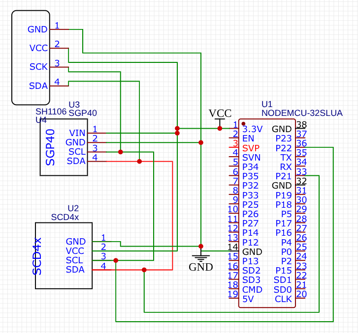
The schematic captures our refined design from the previous iterations, with all the lessons learned about power distribution, I2C connections, and proper grounding integrated into the layout.
Step 2: PCB Layout and Routing
Once the schematic was complete, EasyEDA’s most impressive feature came into play: automatic schematic-to-PCB conversion. With a single click, the tool generated an initial PCB layout with all components placed and basic routing suggestions.
While the auto-layout provided an excellent starting point, I still needed to make manual adjustments:
- Trace Routing: Ensuring signal traces don’t run too close to each other to prevent interference
- Component Placement: Optimizing for both electrical performance and mechanical constraints
- Ground Plane: Creating proper ground planes for stable operation
- Via Placement: Connecting different layers efficiently
The learning curve was gentle enough for a beginner like me, yet the tool provided professional-grade capabilities.
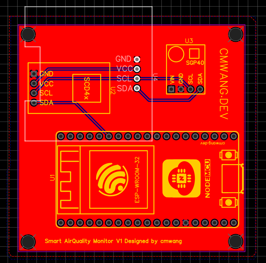
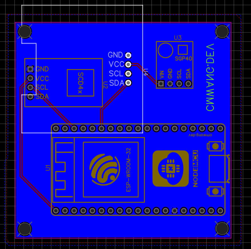
The final design achieved our goals of compactness while maintaining proper electrical design practices. The two-layer board keeps costs low while providing sufficient routing flexibility.
Step 3: Manufacturing - Surprisingly Affordable!
After finalizing the PCB design, I submitted it to JLCPCB for manufacturing. The pricing was genuinely shocking - in the best possible way:
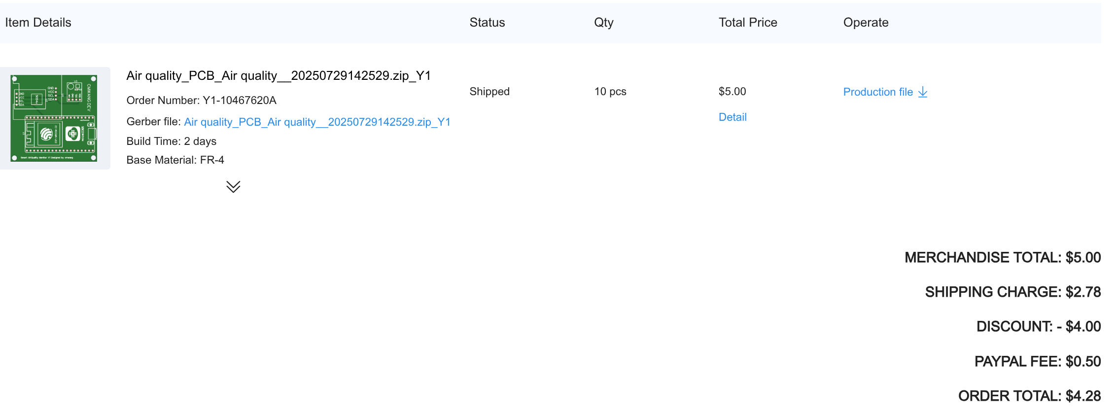
Final Cost Breakdown:
- 10 pieces of custom PCB
- Professional quality with soldermask and silkscreen
- International shipping included
- Total: ~$4 USD (with new customer coupon)
This price point makes experimentation and iteration incredibly accessible. Even if the first design had issues, the cost of multiple revisions would still be minimal.
Manufacturing Progress and Delivery
After placing the order, JLCPCB provided regular updates on the manufacturing progress:
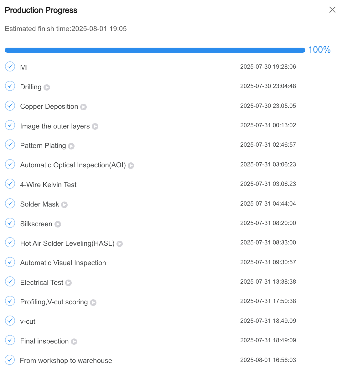
The entire process from order placement to delivery took just 4 days - remarkable considering this included:
- Design review and validation
- PCB fabrication with multiple layers
- Quality control testing
- International shipping from China
When the package arrived, I was impressed by the professional packaging and the quality of the finished PCBs:
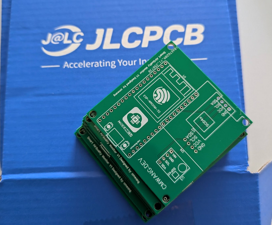
The manufacturing quality exceeded my expectations. The silkscreen was crisp, the soldermask was uniform, and the dimensional accuracy was perfect.
Assembly and Testing
With the custom PCBs in hand, it was time for the moment of truth: soldering the components and testing functionality. Thanks to the improved layout and proper pad sizing, the soldering process was much more manageable than my earlier attempts in Part 5.
After carefully soldering each component:
- ESP32 development board
- SCD41 sensor module
- SGP40 sensor module
- SH1106 display
I flashed the same firmware we developed in previous parts and… it worked perfectly on the first try!
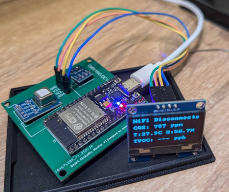
All sensors responded correctly, and the display showed proper readings The months of iterative development and testing with breadboards had paid off - the transition to a custom PCB was seamless.
New 3D Printed Enclosure
With the custom PCB validated, I designed a new enclosure specifically tailored to its dimensions. Using the same OnShape CAD skills developed in Part 5, I created a much more compact design:
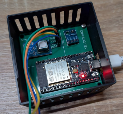
The new enclosure design benefits from:
- Precise Fit: Designed exactly around the PCB dimensions
- Reduced Volume: Significantly smaller than the breadboard version
- Improved Aesthetics: Cleaner lines and professional appearance
Size Comparison: The Transformation
The difference between our original breadboard prototype and the final custom PCB version is dramatic:
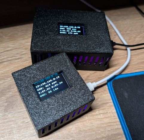
The miniaturization achieved through custom PCB design represents roughly a 60% reduction in volume while maintaining all functionality. This transformation demonstrates the power of moving from prototype to production-ready design.
Modules vs. ICs: Understanding the Trade-offs
While this custom PCB represents a significant improvement, there’s still room for further optimization. Currently, I’m using pre-packaged modules rather than bare ICs:
Current Approach - Using Modules:
- ESP32 Development Board: Includes the ESP32-WROOM-32 module plus USB-to-serial conversion, voltage regulation, and breakout pins
- SCD41/SGP40 Sensor Module: The sensor IC mounted on a small PCB with necessary support components
- SH1106 Display Module: Display controller with integrated voltage regulation and I2C interface
Future Approach - Using Bare ICs:
- ESP32-WROOM-32 Module: Integrate directly onto PCB with custom power regulation and USB interface
- SCD41/SGP40 IC: Mount the bare sensor with custom analog front-end circuitry
- SH1106 Controller: Integrate with custom display driver circuit
Why I Didn’t Use PCBA Service This Time:
Availability: JLCPCB’s component sourcing partner (LCSC Electronics) has excellent stock of common ICs but limited availability of the specific development modules I was using. The variety of form factors and pinouts for modules makes standardization challenging.
Complexity: Moving to bare ICs requires designing additional support circuitry - voltage regulators, crystal oscillators, and protection circuits. While this reduces cost and size, it significantly increases design complexity.
Time to Market: Using modules allowed me to focus on the core functionality rather than getting bogged down in power supply design and RF engineering.
Next Steps: Toward True Production Readiness
This custom PCB version represents a major milestone, but the journey toward a truly production-ready design continues:
- IC Integration: Redesign using bare ICs instead of modules for cost and size optimization
- PCBA Services: Leverage JLCPCB’s assembly services for automated component placement and soldering
- Design for Manufacturing (DFM): Optimize the design for high-volume production
Looking Ahead
As we wrap up this phase of the project, we’ve successfully achieved the core goals outlined in Part 1:
✅ Accuracy First: SCD41 NDIR sensor provides reliable CO2 measurements
✅ Internet Connectivity: WiFi-enabled with Prometheus metrics endpoint
✅ Data Logging & Visualization: Grafana dashboard for historical analysis
✅ Custom Hardware: Professional PCB design with 3D printed enclosure
The next phases will focus on smart home integration and scaling the design for potential small-batch production. Whether you’re interested in IoT development, PCB design, or just following along with this maker journey, the adventure continues!